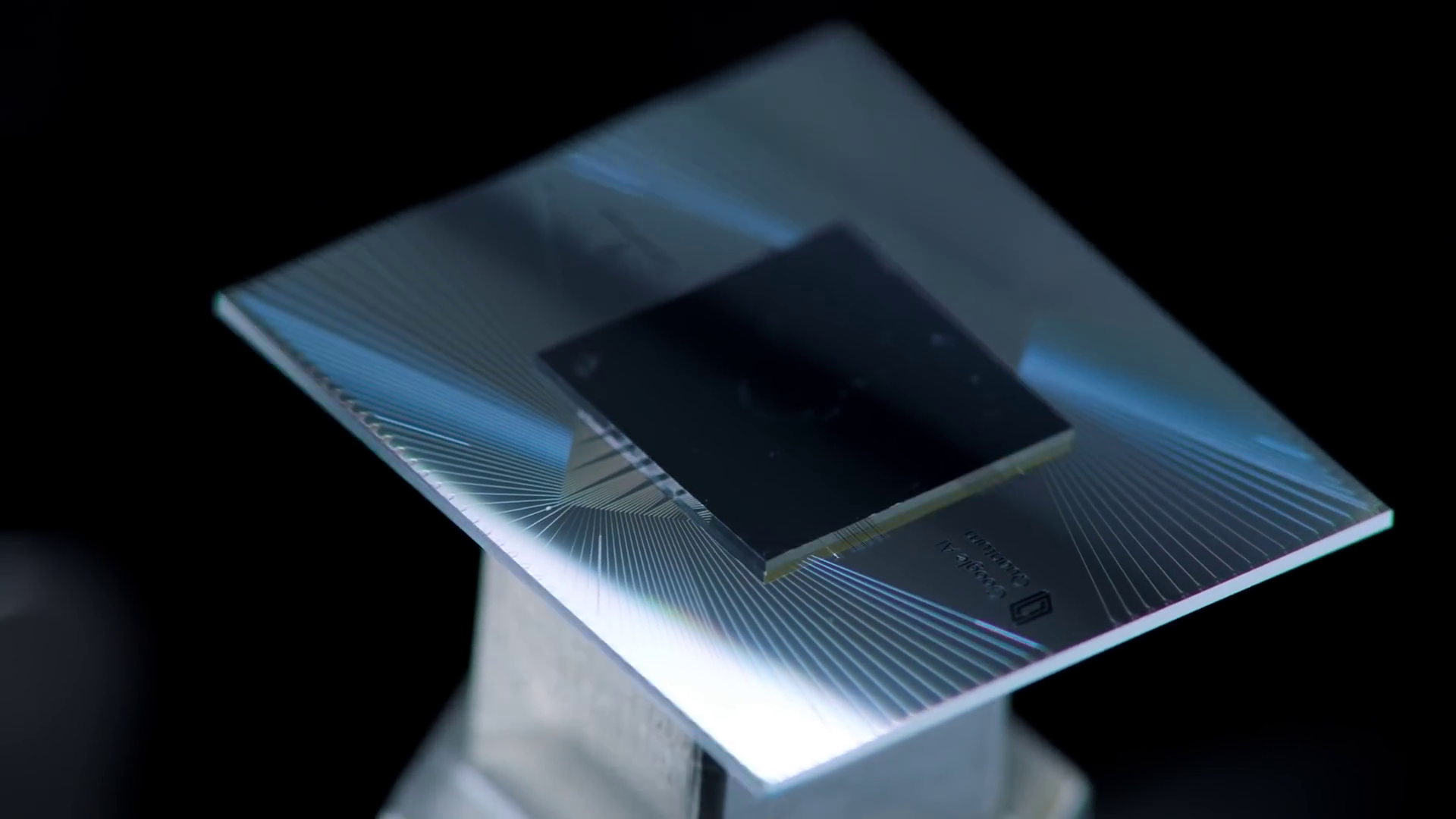
In 2021 and 2022, Google showed that a pod of 4096 custom TPU v4 chips could train machine learning models faster than a comparable system built with Nvidia's A100 GPUs. The numbers came from MLPerf, an independent industry benchmarking consortium that audits and publishes submissions. Google's pod delivered over 1 exaflop of peak AI compute. The A100 system it was measured against was Nvidia's flagship data center GPU from 2020.
The outcome was clear but temporary. Google deployed TPU v4 systems in its cloud regions and continued using them for internal services like Search and YouTube. Nvidia responded in 2022 by releasing its H100 Hopper GPU, which shifted the competitive baseline beyond the A100 comparison. The MLPerf numbers were published and validated, but the broader AI hardware race continued with subsequent chip generations from both companies.
What follows covers what the TPU v4 system won, at what scale, why the architectural differences matter, how Google makes TPU v4 available to customers, and what the outcomes signal for the AI hardware market.

What MLPerf Benchmarks the TPU v4 System Won or Led
Google submitted TPU v4 outcomes to MLPerf for several common benchmarks, including image classification with ResNet-50 and natural language processing with BERT. In those submissions, the TPU v4 pod completed training in less time than the published A100 figures for equivalent tasks. The exact percentage speedups varied by benchmark and configuration, but the trend was consistent: the Google system finished faster.
MLPerf was founded in 2018 to provide a vendor-neutral standard for measuring AI training and inference performance. The consortium includes members from industry and academia. Submissions are audited, and outcomes are published publicly. This gave Google's claims independent credibility.
Nvidia did not issue a formal rebuttal to Google's MLPerf submissions, but the company continued to submit its own figures using newer silicon. The H100 GPU, which Nvidia announced in 2022, subsequently set new records in later MLPerf rounds.
The significance of the TPU v4 outcomes was not that Google beat Nvidia on every metric. It was that a custom chip designed by a cloud provider could compete with and sometimes exceed the performance of Nvidia's dominant data center GPU on standard benchmarks. That was a milestone in the AI hardware race.
Scale of the TPU v4 Supercomputer Configuration
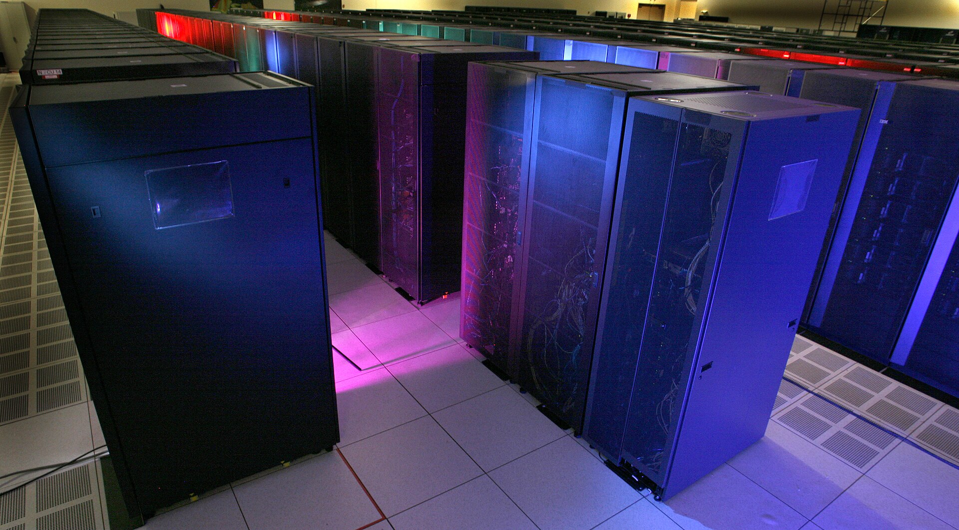
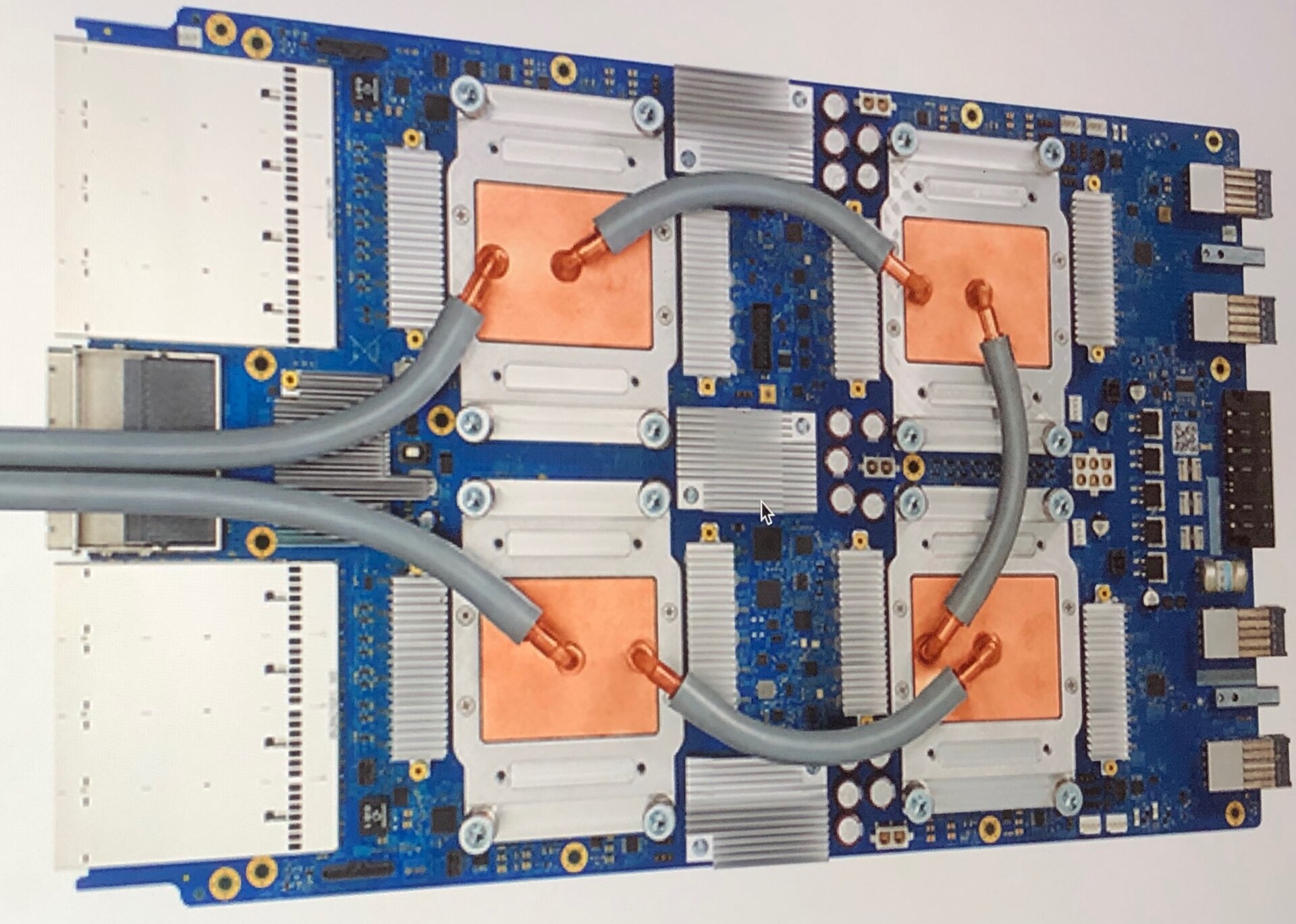
The TPU v4 system that Google submitted to MLPerf was a pod of 4096 chips. A TPU v4 pod is the basic building block of Google's AI infrastructure. Each pod is interconnected with a custom high-speed network that allows the chips to work together on a single training job. Google claimed that a single pod delivered over 1 exaflop of peak AI compute, a measure of raw mathematical throughput for machine learning operations.
The Nvidia A100 system that Google compared against was also a large-scale configuration, though the exact number of accelerators and the topology of the interconnect were not disclosed by Google in the same detail. This makes a direct chip-for-chip comparison difficult. The TPU v4 pod's advantage came partly from the scale of the system and partly from the custom interconnects Google designed to keep the chips busy.
Google did not sell TPU v4 chips directly. Instead, it made them available to customers through Google Cloud, where users could rent TPU v4 pods or slices of pods for their own machine learning projects. This business model contrasts with Nvidia's, which sells A100 GPUs to cloud providers, server manufacturers, and enterprises directly.
Performance Advantage: Speed, Efficiency, or Time to Train
The TPU v4's advantage in the MLPerf benchmarks was primarily in time to train. For a given model and dataset, the Google system completed training in fewer minutes or hours than the A100 system. This is the metric that matters most for many AI practitioners, because faster training means shorter iteration cycles and lower total cost for a given experiment.
Efficiency is a related but distinct measure. It considers the total energy consumed or the cost per training run. Google did not publish detailed power or cost comparisons alongside its MLPerf submissions. The company's public statements emphasized raw throughput and the ability to scale to large models. The TPU v4 pod's custom interconnect and its balanced compute-to-memory ratio were designed to keep utilization high, which indirectly improves efficiency.
Raw speed, measured in teraflops or exaflops, is a specification of the silicon, not a guarantee of training performance. Google's claimed 1 exaflop for a TPU v4 pod was a theoretical peak. The MLPerf outcomes showed that the system could approach that peak on real tasks, which is harder than it sounds. Many accelerators achieve high theoretical throughput only on narrowly optimized kernels.

How Google Makes TPU v4 Available vs. Nvidia's Direct Sales Model
Google does not sell TPU v4 chips. The company uses them internally for services like Search, YouTube, and Gmail, and it offers access to TPU v4 pods through Google Cloud. Customers can provision TPU v4 resources on demand, paying for the compute time they use. This is similar to how cloud providers offer access to Nvidia GPUs, but with a key difference: Google controls the entire stack, from chip design to data center operation to the cloud API.
Nvidia sells A100 GPUs as discrete products. Cloud providers like AWS, Microsoft Azure, and Google Cloud itself buy A100 chips and integrate them into their own infrastructure. Enterprises can also buy A100-based servers directly from Nvidia's hardware partners. This direct-sale model gives Nvidia a broader market but less control over how the chips are deployed and optimized at scale.
For customers, the choice between TPU v4 on Google Cloud and A100 on a cloud provider depends on workload, budget, and lock-in considerations. TPU v4 is only available on Google Cloud, while A100 is available on multiple platforms. Google's TPU v4 pod pricing was not directly comparable to A100 instance pricing at the time, because the configurations and software stacks differed.
Architectural Differences Between TPU v4 and A100
Specialization vs. generality
The TPU v4 is a custom ASIC designed by Google specifically for machine learning. It is built on an unspecified process node, though industry analysts generally place it at 7nm or similar. The chip is optimized for matrix operations, which dominate deep learning training. It includes a large systolic array for multiply-accumulate operations and a custom interconnect that allows pods to scale efficiently.
The Nvidia A100 GPU, introduced in 2020, is built on TSMC's 7nm process. It is a general-purpose GPU that can handle graphics, scientific computing, and AI tasks. The A100 includes Tensor Cores, which are specialized units for matrix math, but the chip must also maintain compatibility with the broader CUDA ecosystem. This generality imposes some overhead compared to a purpose-built ASIC like the TPU v4.
Scaling architecture
The key architectural difference is specialization. The TPU v4 has no display outputs, no general-purpose shader cores, and no legacy graphics pipeline. Every transistor is there to accelerate machine learning. The A100, by contrast, is a Swiss Army knife. That makes it more flexible but potentially less efficient for pure training at scale. The TPU v4's custom interconnects also give it an advantage in scaling to 4096 chips without hitting communication bottlenecks.
The Competitive Baseline Shifted After the Results
Google's TPU v4 MLPerf outcomes were a milestone, but the competitive landscape did not freeze at that moment. Nvidia released its H100 Hopper GPU in 2022, built on TSMC's 4nm process with a new transformer engine and faster memory. The H100 set new MLPerf records in subsequent rounds, surpassing the TPU v4 figures on several benchmarks.
This is the normal pattern in the AI hardware race: each generation leapfrogs the previous one. Google continued to deploy TPU v4 systems in its cloud regions and for internal services. The chips power Search, YouTube, and Gmail, where they handle both training and inference. Google has also developed subsequent TPU generations, though the company has not disclosed details about TPU v5 or later versions in the same level of detail as v4.
The broader lesson from the TPU v4 versus A100 comparison is that custom silicon can compete with merchant silicon in AI training, but the advantage is temporary. Nvidia's rapid release cadence and its dominance of the AI software ecosystem mean that any single benchmark victory is soon overtaken. For operators and investors, the relevant question is not which chip won in 2021 but which company can sustain the pace of improvement.