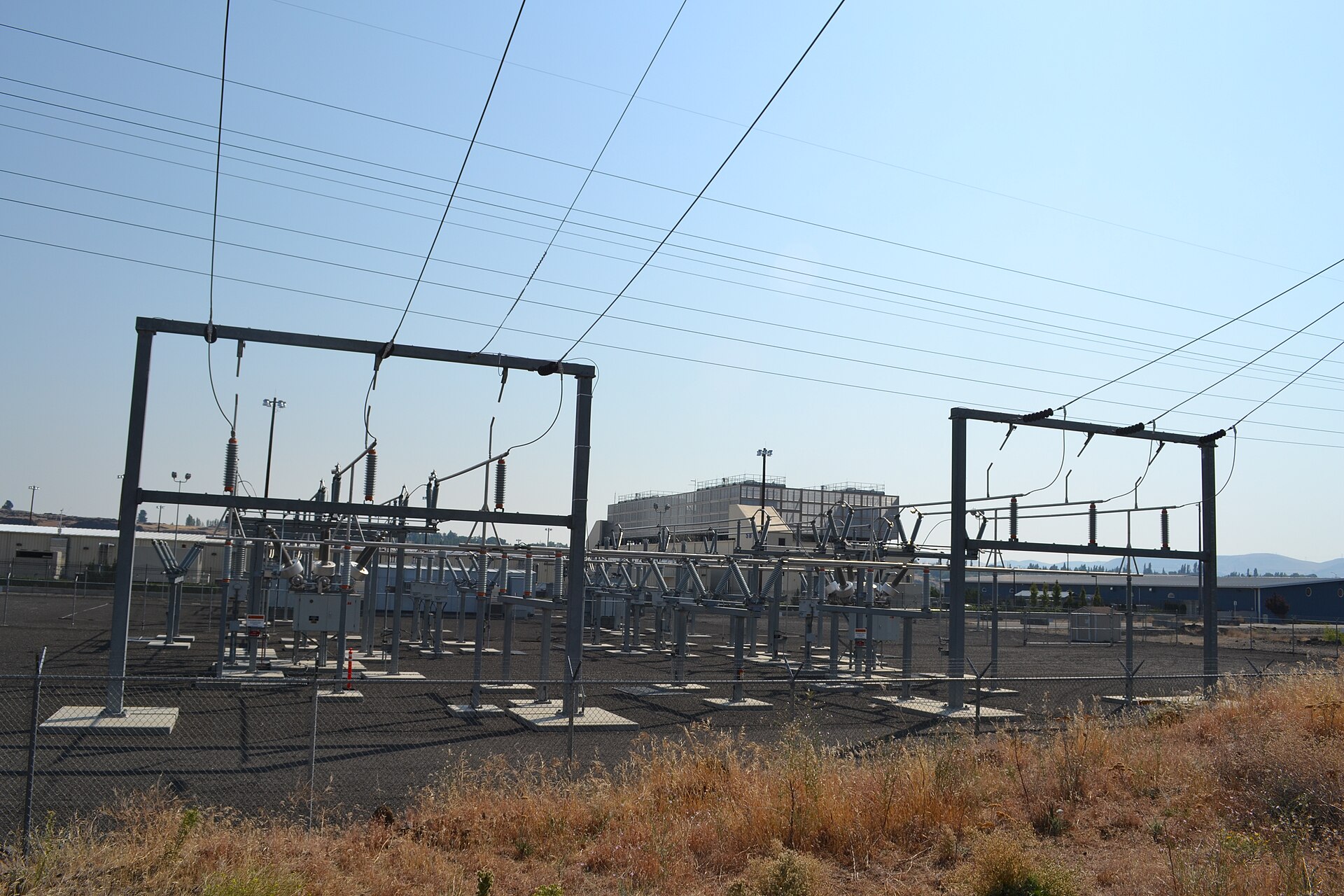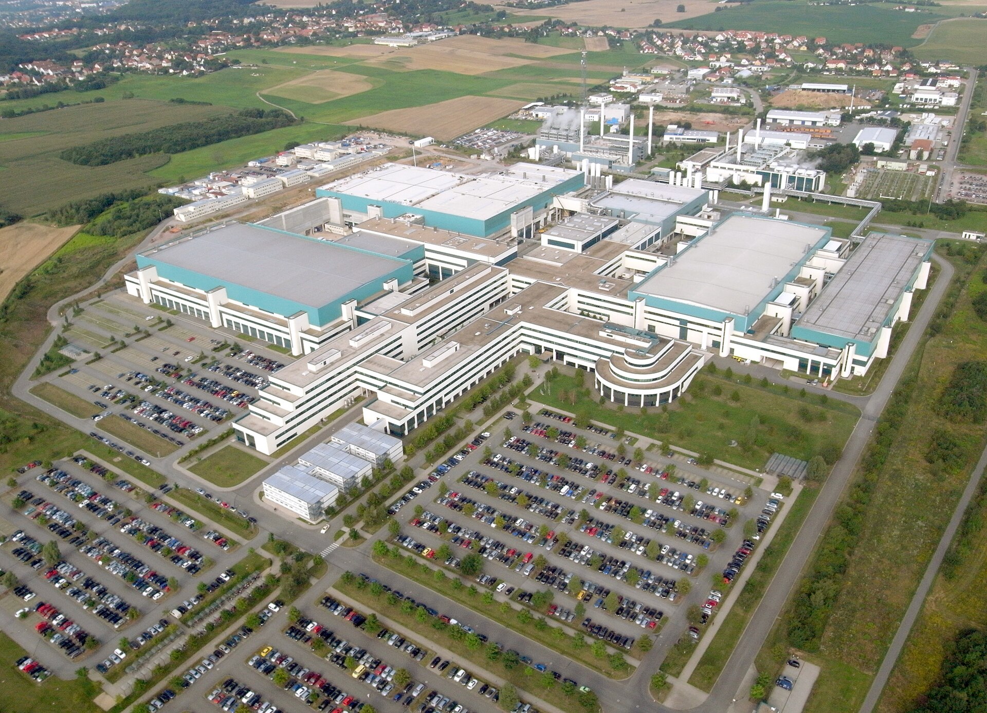
GlobalFoundries officially opened its new $4 billion semiconductor fabrication plant in Singapore on September 12, 2023. The facility is already operational and ramping production.
Located on the firm's existing Woodlands campus, the fab makes chips on 300mm wafers. It adds manufacturing heft at a moment when the chip industry is still working through supply constraints. The Singapore Economic Development Board (EDB) was a key partner. The $4 billion total includes contributions from both GlobalFoundries and government co-investment, though the exact split is undisclosed.
The foundry first announced the project in June 2021. The opening came just under two years after its Nasdaq IPO in October 2021. GlobalFoundries is headquartered in Malta, New York, and the Singapore expansion is one of several major investments the firm has made since going public. The fab targets automotive, communications infrastructure, and industrial chips.

Investment Structure and Government Support
The $4 billion outlay ranks among the larger single-fab commitments in Singapore's chip ecosystem. The EDB's involvement signals the government's determination to keep the city-state a manufacturing hub for advanced chips, even as other nations compete for fabrication investments with subsidies and tax breaks.
GlobalFoundries did not disclose the precise split between its own capital expenditure and Singaporean co-investment, nor whether the government holds any equity in the facility. The EDB's partnership role included shepherding the project's approval and almost certainly providing an incentive package, standard practice for large industrial investments in Singapore.
Building on the existing Woodlands campus let the firm sidestep greenfield timelines. It could tap ready-made infrastructure, utilities, and a trained workforce.
Manufacturing Technology and Process Nodes
GlobalFoundries has not publicly named the exact nanometer nodes the Singapore fab will run. Its technology portfolio spans mature and advanced processes, and the facility is expected to produce chips across several nodes rather than a single generation.
The fab processes 300mm wafers, the industry standard for volume production. That wafer size delivers better economies of scale than the older 200mm format, which lingers for some specialty chips but struggles to compete in high-volume manufacturing.
GlobalFoundries positions itself as a specialty foundry. It does not compete head-to-head with TSMC or Samsung at the leading edge. Instead, it focuses on proven, reliable processes for uses where performance, power efficiency, and cost are balanced. The Singapore plant will likely run GlobalFoundries' established platforms rather than introduce entirely new nodes.
Production Capacity and Output
GlobalFoundries has not disclosed the fab's exact capacity in annual wafer starts. The firm says the facility adds significant volume to its global network but has offered no specific number.
Actual output will depend on product mix and ramp-up pace. The facility is operational as of September 2023 and is ramping production, a process that typically takes 12 to 24 months to reach full capacity as equipment is installed, qualified, and stabilized. GlobalFoundries has not given a timeline for hitting full production volume.
Employment and Workforce
GlobalFoundries has not disclosed a precise headcount target for the new Singapore fab. The firm says the facility will support high-skilled roles but has not named a specific figure. The operation will draw on Singapore's existing pool of chip engineers and technicians, plus new graduates from local universities and polytechnics.
Semiconductor fabs are capital-intensive, not labor-intensive. A project of this scale might directly employ several hundred to over a thousand people, but the foundry has confirmed no range. The roles span process engineers, equipment technicians, facilities operators, and supporting functions in quality, logistics, and management.
Strategic Context After the IPO
GlobalFoundries went public on the Nasdaq in October 2021, months after announcing the Singapore fab. The IPO raised capital for expansion, and the Singapore project is among the largest single investments the firm has made as a public entity.
The post-IPO strategy: grow manufacturing footprint in regions with stable business climates and government backing, while diversifying geographically. Singapore delivers a skilled workforce, established infrastructure, EDB partnership, and a location serving customers across Asia.
The global chip shortage that began in 2020 and persisted through 2023 drove intense demand for additional fabrication capacity, especially on mature nodes for automotive, industrial, and communications uses. GlobalFoundries' Singapore expansion is positioned to capture that demand, particularly from customers wanting to diversify supply chains away from heavy concentration in Taiwan and South Korea.
End-Market Applications and Customer Base
Automotive
Automotive chips are a critical segment for GlobalFoundries. The car industry was hammered by the semiconductor shortage, and many manufacturers have since pursued long-term supply agreements with foundries. Automotive-grade chips demand high reliability and long product lifecycles, a profile that fits the specialty foundry model.
Communications and Industrial
Communications infrastructure chips go into 5G base stations, networking equipment, and data center connectivity. Industrial uses cover factory automation, power management, and sensors. The Singapore fab is not expected to serve smartphones or high-performance computing; those segments belong to leading-edge foundries like TSMC and Samsung.
Customer Mix
GlobalFoundries has not publicly named specific customers for the Singapore plant. Its customer base mixes large multinational chip firms and fabless designers. The Singapore location positions the fab to serve clients in Southeast Asia, China, and other parts of Asia more efficiently than the firm's plants in the United States or Europe.
Key Facts
- Company Headquarters: Malta, New York, USA
- Investment Amount: Approximately $4 billion
- Location: Woodlands, Singapore (existing campus)
- Official Opening Date: September 12, 2023
- Wafer Size: 300mm
- Key Government Partner: Singapore Economic Development Board (EDB)
- IPO Date: October 2021 (Nasdaq)
- Announcement Date: June 2021
- Status: Operational and ramping production